


Important Links
Product Page
Store Page
Assembly Instructions
Bill of Materials
Schematic
Capacitor and Resistor Lookup Guide
Welcome to the 555 Timer Assembly Instruction! This simple circuit is very powerful and has a ton of applications. Let’s get started!
Component Layout

Check to make sure that you have all of the components included in the kit. Not only will this help you finish the circuit, but it will familiarize you with each component.
For these instructions, a DC jack is used. However, this component is not necessary to power your circuit and it is not included in kits.
Alright, let’s get started building!
Assembly
Attention: Changes may occur after the Assembly Instructions are created and the photos may not reflect those changes. Always use the BOM to verify the placement of components.
On-board Components

Insert the IC Socket, and the 1k resistors into the PCB. Use the picture above for a reference.
Bend the leads on the back, and solder the components into place. Then clip the leads!

The capacitors are placed as shown. C1 is a polarized electrolytic capacitor, and it’s lead placement is important. The colored stripe on the side of the electrolytic capacitor denotes the negative lead. Place the shorter negative lead into the circle through-hole, and the longer lead into the square (positive) through-hole. C2 and C3 are ceramic capacitors; their placement does not matter.
My personal preference is to insert multiple components before any soldering takes place. Make sure your soldering joints are clean before you clip any leads from the capacitors or the resistor.

Insert the potentiometer as shown in the picture above, and solder the pin-connections.
The potentiometer can also be wired. Just make sure to align it in the same way.
When installing the pot, some pots come with nubs near the shaft that may get in the way of installing the circuit into a case. Check for a nub and clip as necessary.
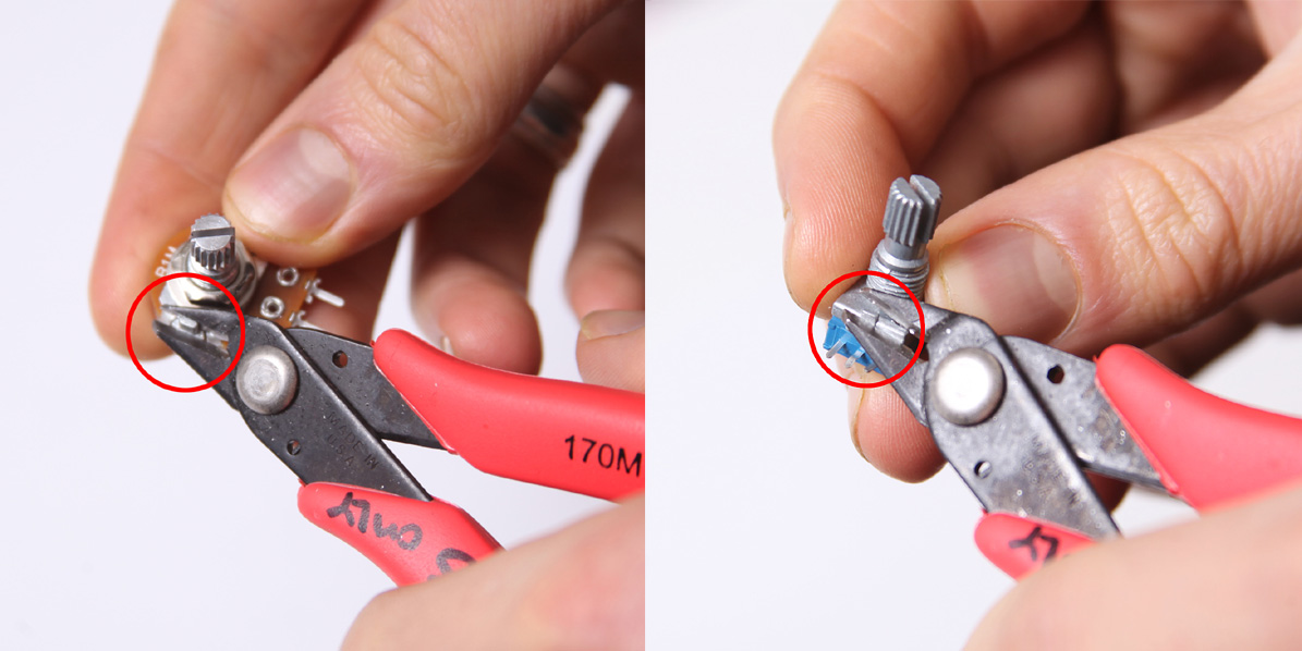
Don’t forget to cut the nubs on the potentiometers as neccesary.
Wired Components
The remaining components of the 555 Timer circuit are attached to the PCB via wires. Use longer wires than you need when soldering to the component. Wire can always be cut; desoldering short wires and resoldering new wires to the PCB and component is a very frustrating error that can be avoided.

The jacks are very easy to solder to the board.
The red wire of the battery jack goes to the V+ PCB position and the black wire goes to the GND position.

If you are using a DC jack with your circuit, read on.
These are pictures from the Synthrotek Dev Board Assembly Instructions. They will explain how to wire up a 9volt DC jack along with the battery jack for your 555 timer.

Use this picture for wiring a center positive power supply. The red and black wires are the battery jack connections.
The top through-hole on the PCB where the DC jack is connected reads “Vcc” which is the same as V+ on the 555 PCB.
The through-hole below that is the GND. Wire up the 555 Timer PCB in the same manner.

Use this picture for wiring a center negative power supply. The red and black wires are the battery jack connections.
Mods/Applications
If you are new to electronics, you may not fully understand the point of this circuit. That’s totally OK and we are going to show you what you can do with it. There’s more to it than just flashing an LED on and off!
The circuit layout is for a 555 timer in astable mode. Basically, this means that you will have a continuous transition from a high voltage level (determined by and slightly less than your supply voltage) to 0V at a certain frequency (number of times per second). In digital circuits, this is known as a clock pulse and is very important for timing or triggering events. In fact, our 8/10 step sequencer and 16 step sequencer both utilize an astable 555 timer circuit!
For more info, check out this link. They do a great job of explaining the circuit as well as showing how to calculate frequency and component values.
Controlling a Relay
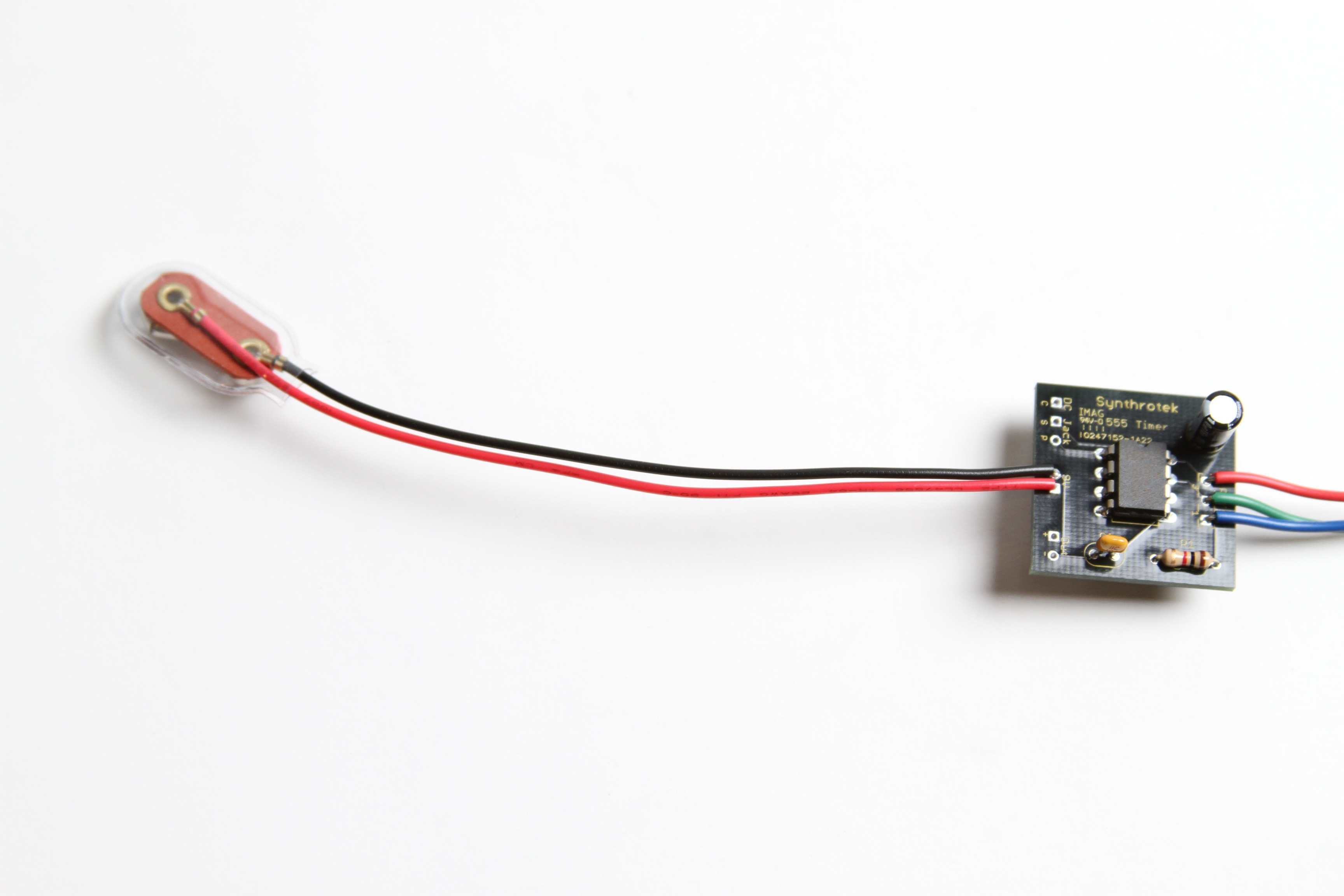
CV Input
Circuit Bending
8 Comments