


Important Links
Product Page
Store Page
Assembly Instructions
Bill of Materials
Schematic
Capacitor and Resistor Lookup Guide
Welcome to Synthrotek PT2399 Dev Delay Assembly Instructions! This step-by-step guide will take you through the whole circuit-building process.
Component Layout
The first step in any successful DIY electronics project is to make sure that you have all of the parts and know their reference ID for proper board placement. Check the contents of your kit against the BOM before you begin. If you’re missing anything, send us an email and we’ll get it out to you ASAP.

Got all of your components? It’s time to start building.
Assembly
The first part of our build will be for components that are soldered directly to the circuit board. This makes the build process easier than having to deal with wires and floating potentiometers getting in our way while we solder sensitive components.
Attention: Changes may occur after the Assembly Instructions are created and the photos may not reflect those changes. Always use the BOM to verify the placement of components.
IC Sockets/Resistors

Insert the resistors into their respective PCB positions and solder them to the board. Use the BOM to identify resistor placement. Don’t worry too much about damaging resistors with your soldering iron; resistors are not fragile components.
Insert the IC Socket into the PCB as show above. Make sure that you align the notch on the socket with the notch on the silk screen. Next place the IC into the socket as well and again align the notch on the IC with the notch on the socket. Do this carefully as to not bend the IC pins.
Capacitors

There are two different types of capacitors in this circuit. Electrolytic capacitors (C2, C3, C9, C13, and C14) are polar components and their pcb placement matters. The shorter lead and the band on the body identifies the negative lead, which will be inserted into the circle through-hole. The positive lead will be longer and should be inserted into the square through-hole.
Polarity is not an issue with the remaining ceramic capacitors. Just be sure the component values are identified before soldering them; some of them look very similiar and the codes printed on their bodies are the only way to identify them.
Note: (C15, C17) could be either electrolytic or ceramic capacitors.
Voltage Regulator

Solder the voltage regulator for U2 as shown in the picture. Align the flat side with markings on the board.
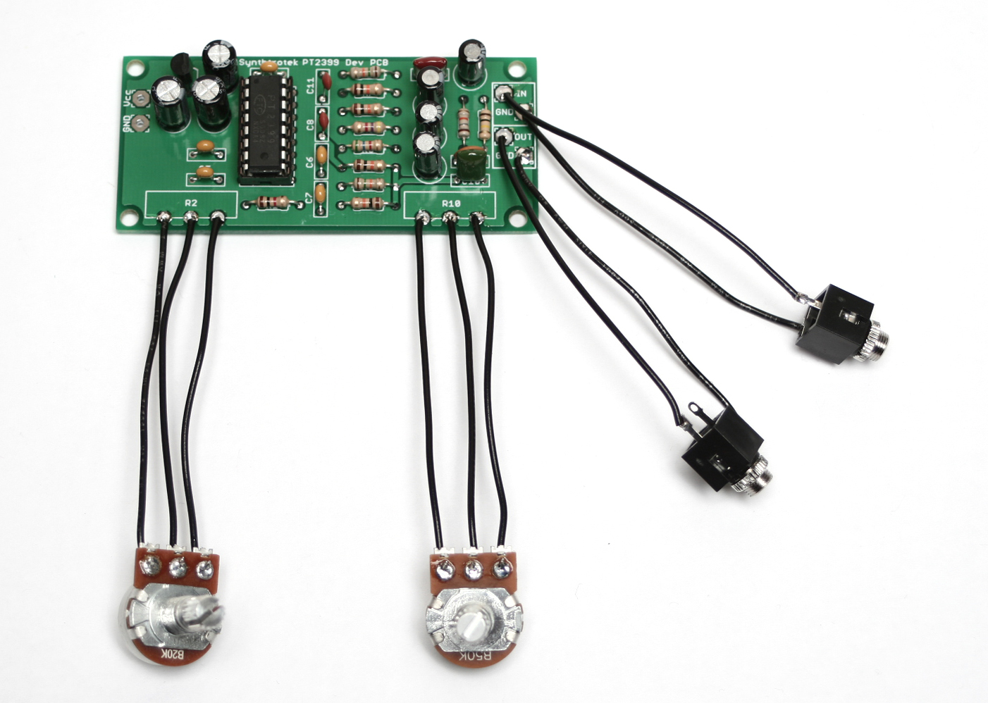
Potentiometers & Audio Jacks
Solder wired leads to a B50K potentiometer, B20K potentiometers, and both audio jacks. Connect these components to their respective locations using the photo below for reference.
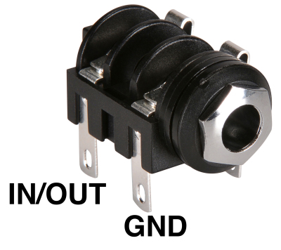
1/4″ Jack Wiring
1/4″ Metal Audio Jack Wiring – Sleeve is Ground, Tip is IN/OUT
You may opt to mount R2/R10 directly to the PCB, but be aware that this will cause the potentiometers to increase mix/depth when turning counterclockwise.

Some pots come with nubs near the shaft that may get in the way of installing the circuit into a case. Check for a nub and clip as necessary.
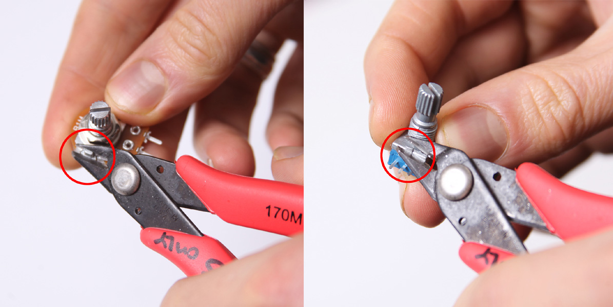
Don’t forget to cut the nubs on the potentiometers as necesary.
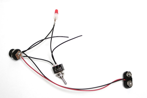
DC Jack, Power Switch, LED, and 9V Clip
For 9V center negative wiring, connect the ‘S’ contact of the D/C jack to one of the contacts on the SPST switch – this switch will control current flowing to both the circuit and power LED. Solder a 1K resistor to the positive (round edge) lead of the LED. Solder two wires to the unused SPST switch contact, connecting one to the remaining contact on the 1K resistor. Solder two wires and the negative lead on the battery clip to the ‘P contact of the D/C jack, connecting one of the two wires to the negative (flat edge) lead of the LED. Connect the remaining wire running from the SPST switch to the ‘VCC’ contact on the delay, and the remaining wire from the ‘P’ contact to the ‘GND’ contact on the delay. Solder the positive battery clip lead to the ‘C’ contact on the DC jack. You may optionally omit the 9v battery clip if desired.
DC JACK WIRING – DEV DELAY
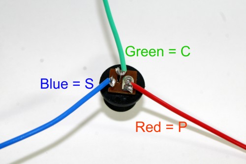
DC Jack Pinout
Warp, Feedback, and Feedblast Mods
Solder wires to both contacts on one of the momentary switches and solder a 200k resistor to one contact on the other momentary switch. Attach wires to the resistor, remaining contact on the momentary switch, and pins 2/3 on the 50k potentiometer. The momentary switch with the resistor will be used for the feedblast mod, the other momentary for the warp mod, and the 50k pot for the feedback mod.
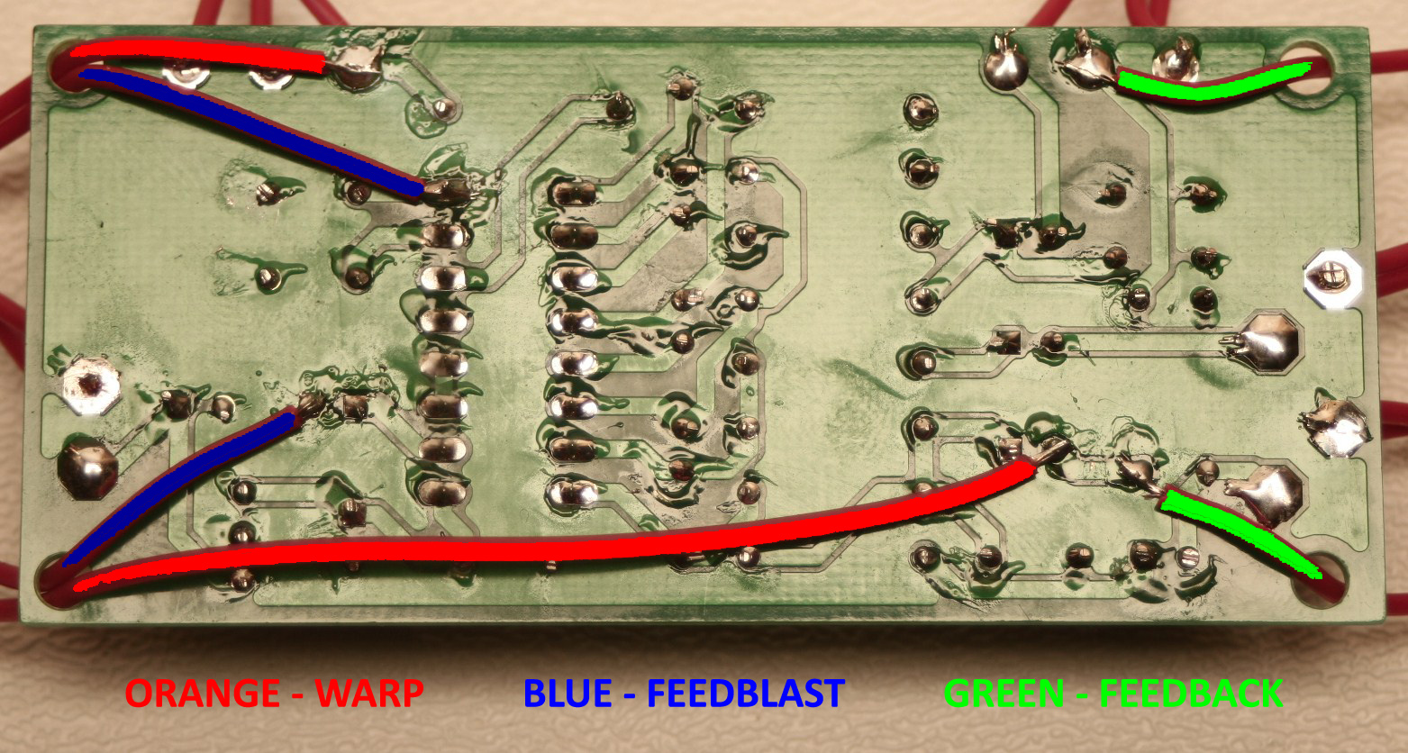
Connect the appropriate components to the following locations:
Feedback: R10 (2) –> 50k pot (2), R11 (via adjacent C17) –> 50k pot (3)
Feedblast: Pin 8 (IC Socket) –> C3 (-)
Warp: R2 (1) –> C15 (-)
Pin 2 on the 50K feedback pot must be connected to pin 2 of R10, and the momentary switch with the 200k in-line resistor should be used for the feedblast mod. Switch polarity has no effect on the feedblast or warp mods. It may be beneficial to route wires through the holes in the corners of the board to provide strain relief for the delicate mod connections.
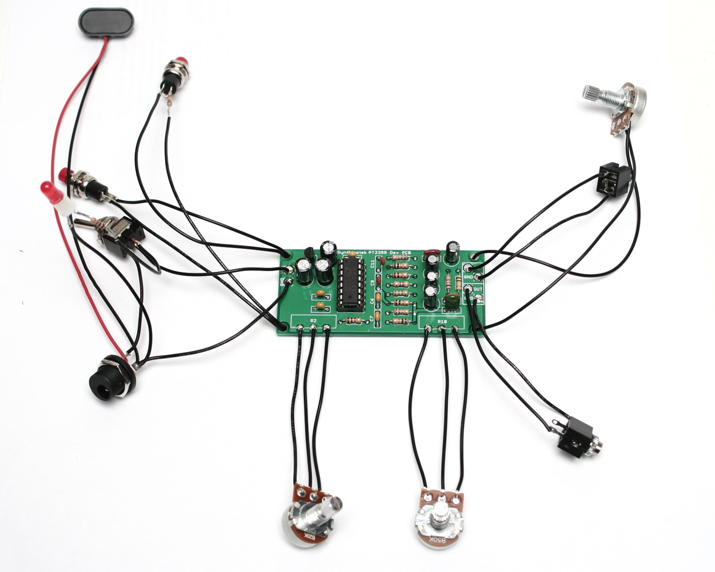
Completed Project
83 Comments