


Important Links
Product Page
Store Page
Assembly Instructions
Bill of Materials
Schematic
Capacitor and Resistor Lookup Guide
Welcome to the 4093 NAND Synth Assembly Instructions – let’s get started!
BOM Layout

NAND Synth Kit
The first step in any successful electronics project is to make sure that you have all of the parts necessary to complete the circuit.
Check your kit against the BOM. If you are missing a part, we’ll send it to you free of charge.
Attention: Changes may occur after the Assembly Instructions are created and the photos may not reflect those changes. Always use the BOM to verify the placement of components.
PCB-Mounted Components

Begin by locating the component identifiers for R1, R2, R3, R4, and R5. Insert the resistors and solder all components onto the PCB.

Next solder the IC socket to the PCB and insert the 4093 IC, aligning the notch in the socket/IC with the corresponding marking on the silkscreen.

Our next step will be to insert all capacitors through the PCB and solder into place. Align the stripe/shorter lead on the the 2.2μF and 100μF capacitors with the negative via on the silkscreen. The 0.1μF capacitors are not polarized and may be inserted in any orientation.
Wired Components
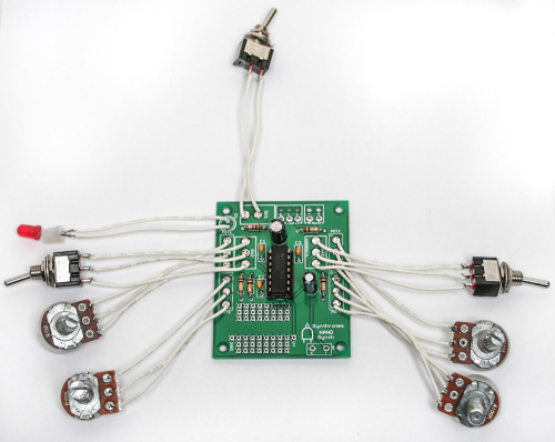
The next major step in our project assembly will be the wired components. Attach wires to all of the potentiometers, switches, and jacks beforehand. This will save time and the construction of the circuit will be much simpler.
Solder the leads connected to the leftmost and rightmost contacts on the potentiometers to terminals 1 and 3, respectively. See the photo below for reference orientation:

When installing the pot, some pots come with nubs near the shaft that may get in the way of installing the circuit into a case. Check for a nub and clip as necessary.
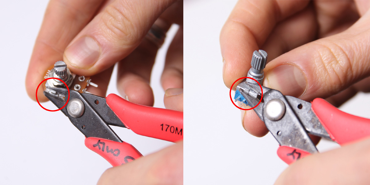
Don’t forget to cut the nubs on the potentiometers as necessary.
Next solder the leads running from the SPDT and SPST switches to the appropriate terminals on the PCB.

Attach wire leads to the LED, optionally inserting the plastic LED mount of the legs of the LED prior to soldering. Solder the LED leads to the terminals on the PCB – connect the wire running from the leg closest to the flat edge of the LED to the corresponding contact as indicated on the silkscreen.
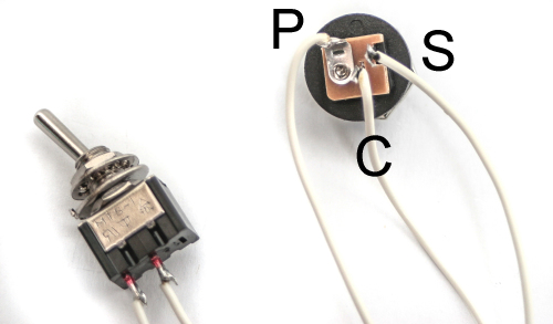
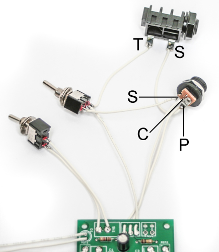
Proceed to solder the leads running from the output jack to the ‘T’ and ‘S’ contacts on the PCB – see the photo below for reference:
See the following photo if you are installing an 1/8″ jack:
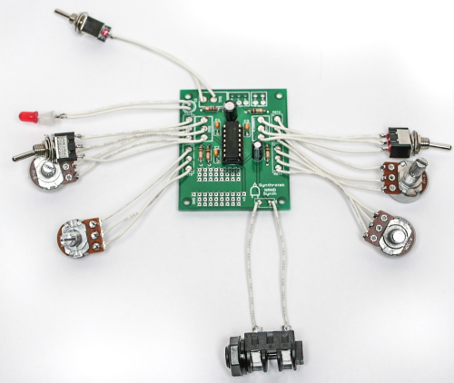
Next insert the wire leads connected to the DC jack through the strain relief holes in the PCB and solder into place.
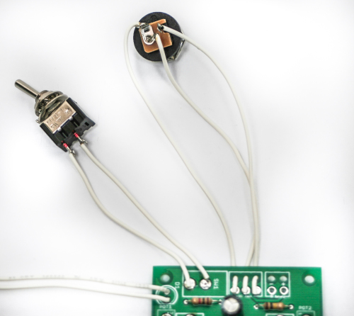
The P, C, and S terminals on the PCB correspond to the following contacts on the DC jack:
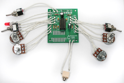
Optional: install the 9v battery clip by inserting the leads through the strain relief holes – connect the red lead to the positive (+) contact and the black lead to the negative (-) contact. If you do not want to install the 9V DC jack and only install the 9V battery clip, short the S and C pins for the 9V DC Jack as shown in the photo below:
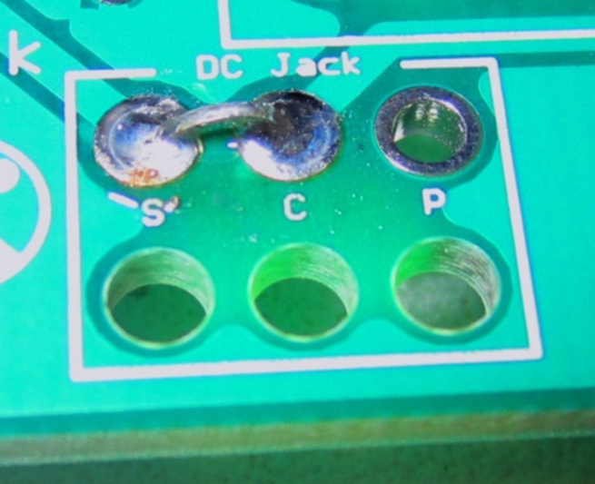
Short these contacts to get the circuit to work without the 9V DC Jack
Completed Project
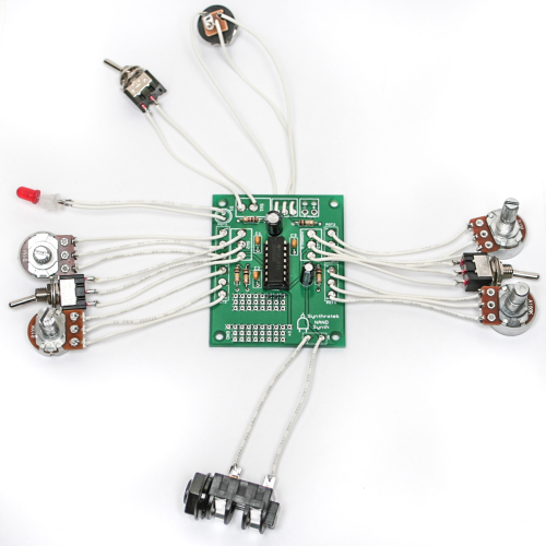
Congratulations, your NAND Synth circuit is complete! Connect your circuit to a power source and amplifier to test if it’s operational. If not, go back through the steps in these instructions and look for any mistakes. When you have a fully functional circuit, check out the mods section below for ways to modify your circuit. Have fun with your hand-made NAND Synth!
Mods
CV Input
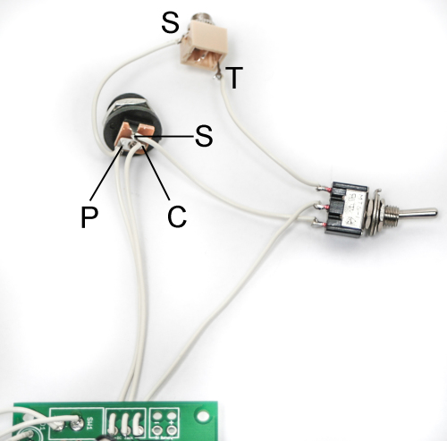
This mod allows you to use an external control voltage signal to alter the NAND Synth’s output pitch. The additional mono jack, SPDT switch, and wire necessary to perform this mod are included in all retail kits and specified in the BOM. Begin by building up the NAND according to the instructions, but omit the DC jack.
Solder wire between the tip contact of the mono jack jack and one of the two outer solder lugs on the SPDT switch. Connect the other outer lug to the ‘S’ contact on the DC jack, and the middle lug to the ‘S’ contact on the PCB. Solder wire leads from the mono jack sleeve contact and ‘P’ contact on the PCB to the ‘P’ contact on the PCB. Finally, connect a wired lead from the ‘C’ contact on the DC jack to the ‘C’ contact on the PCB.
The DC jack, additional mono jack, and SPDT switch should be wired similarly to this reference photo:
See the following photo if you are using an 1/8″ jack:
Alright, you’re finished! Now go grab your sequencer and start making some noise!
Dive Bomb
This mod allows you to momentarily cut the power off to the circuit, resulting in an an awesome-sounding Dive Bomb effect. It’s a simple mod and only requires a SPDT switch and some wire. For maximum playability, we suggest using a momentary pushbutton SPDT switch.
These instructions use the 9V battery source for these instructions. If you choose to use this mod with both jacks, you will need a separate pushbutton switch for each power source. Because of the PCB layout, this mod is only able to be used with one power source.
Locate the red wire of the 9V Battery Jack, clip it halfway down the length of the wire, and strip the ends (if you are using the DC Jack instead, cut the wire connected to the DC Jack through-hole labeled ‘S’).
Attach two long wires to the stripped leads and solder.
Next, find the COM (common) and N.C. (normally closed) connections on the switch. Connect the newly-attached wires from the 9V battery adapter to these solder lug positions on the switch (it does not matter where each goes).
That’s all there is to it! Now your NAND Synth circuit is capable of Dive Bombing like a guitarist!
Note: The length of the Dive Bomb can also be shortened or lengthened depending on the capacitor value used. More on this coming soon!
38 Comments